How To Improve Your PCB Layout - VIAs
Optimize Your PCB Design! Setting Up Via Styles in Altium | Ashraf ExplainsПодробнее

Tutorial - Custom DIY Keyboard Design and Build | Part 5: PCB Layout ImprovementПодробнее

Optimize Your PCB Design: The Secret to Lower Inductance!Подробнее

Nice Use of Thermals! 1 Min PCB Design ReviewПодробнее

High-Speed PCB Via Design and Manufacturing | Sierra CircuitsПодробнее

JLCPCB, Easyeda 5 tips for better PCB designПодробнее

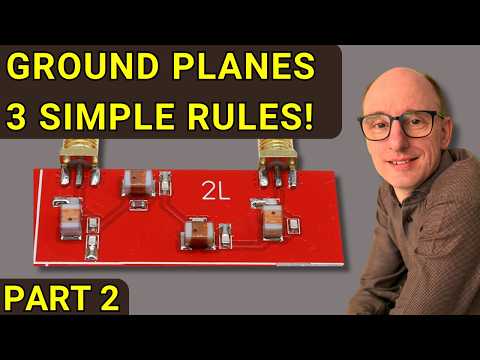
Flawless PCB design: 3 simple rules - Part 2Подробнее
When to Apply Thermal Relief Pads to Your PCBПодробнее

Как интегрировать пропускные переходы в дизайн печатной платы HDIПодробнее

Swiftly Resize Tracks, Vias, Holes & More Using the DEX PCB DesignerПодробнее

STM32 Fanout: Through-Holes vs. HDIПодробнее

What are Stitching Vias? | PCB KnowledgeПодробнее

Mastering High-Speed Protocols: Diving into Modern PCB DesignПодробнее

6 Horribly Common PCB Design MistakesПодробнее
How to Use Blind and Buried ViasПодробнее

How to Reverse Engineer a PCB from Gerber FilesПодробнее

Altium Designer Tutorial 28: Altium Design rule for Via under SMD PAD.Подробнее
