CMOS NAND Gate Stick Diagram: Circuit, Design & Working
CMOS as AND gate Explanation। Working, Truth Table, Circuit Diagram। M.sc physics। NET jrf physicsПодробнее

CMOS as NOR Gate Explanation Circuit Diagram। Working , Truth Table। net jrf physics, m. sc physicsПодробнее

CMOS as NAND Gate Explaned Circuit, Working, Truth Table in Digital Circuit। M.sc Physics, net jrfПодробнее

CMOS AS A NOR GATE | COMPLEMENTARY METAL OXIDE SEMICONDUCTOR| DIGITAL ELECTRONICS SECRETS OF PHYSICSПодробнее

Stick Diagram of Two Input CMOS NOR Gate: Quick and EasyПодробнее

STICK DIAGRAM | ECT304 VLSI CIRCUIT DESIGN | MODULE 5 | KTUПодробнее

CMOS Logic Design: Stick Diagrams, Euler Graphs, and Combinational Gates! 🔍🔌 #CMOSПодробнее

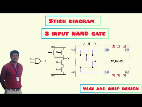
Stick Diagram for 2 Input NAND gate in CMOS LOGIC VLSIПодробнее

Stick Diagram for CMOS NAND gateПодробнее

Stick Diagram for CMOS NOR GateПодробнее

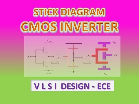
Stick Diagram for CMOS InverterПодробнее
Two Input CMOS NAND GATE in VLSI DESIGNПодробнее

stick diagram for 2 input nand gateПодробнее
Euler's Graph and Stick Diagram in VLSI Design || Learn Thought || S Vijay MuruganПодробнее

Stick diagram for Boolean Expression Using NMOS transistor | VLSI Design | S Vijay MuruganПодробнее

Stick Diagram of a Boolean Function using PMOS | VLSI Design | S Vijay Murugan | Learn ThoughtПодробнее

CMOS Stick diagram RulesПодробнее

Pseudo nMOS logic | CMOS Logic | VLSI | Lec-55Подробнее

2 input NAND gate stick and mask layout design using cmos technology, How to design stick and maskПодробнее

CMOS | 2-input NAND and NOR gates | Layout diagram | VLSI | Lec-34Подробнее
